Quietly Struck Technology Triggered A Major Change In The Photovoltaic Industry!
17/03/2020Quietly Struck Technology Triggered A Major Change In The Photovoltaic Industry!
A butterfly effect caused by upstream technological changes is spreading to the entire photovoltaic industry.
Every technological change in the photovoltaic industry is accompanied by changes in the industry, and every change, like a big wave of sand, screens out new winners.
The photovoltaic industry in 2020 is also entering this moment of change. Parity on the Internet, market-oriented changes, overseas competition ... all of which put forward higher requirements for product technology.
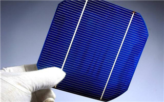
The first technological change was the silicon wafer upstream of photovoltaics.
In recent months, leading wafer manufacturers have almost invariably set off a wave of technological change around "large-size" silicon wafers, and a technology iteration that may affect the entire photovoltaic industry is coming.

01 Who is making large size silicon wafers?
At the beginning of the resumption of work in the photovoltaic industry, many companies couldn't wait to announce plans to expand production. This year's development focus gradually emerged.
On February 20, Zhonghuan shares announced a fundraising announcement. The total amount of funds to be raised does not exceed RMB 5 billion for large-scale silicon wafer projects.
This is already the case of Zhonghuan Co., Ltd. has repeatedly oversized large-size silicon wafers since the second half of last year. It is understood that the current five-phase project of Zhonghuan Co., Ltd. has a capacity of 210mm large-size silicon wafers, and the investment is evident.
In addition to Zhonghuan, Longji also began to increase the size of large-size silicon wafers last year. However, unlike Zhonghuan, Longji's main silicon wafer size is 166mm. At the same time, Longji's existing battery chip and module production lines have also begun to transform and build adaptations. Production line of this size.
It is no coincidence that two companies that once ranked first and second in the global silicon wafer industry are focusing on large-size silicon wafers at the same time. Although the two companies have different technology choices, at least it can be explained that the upstream silicon wafer field of photovoltaics has entered the era of large silicon wafers.
Of course, the changes in the industry naturally attracted the attention of other companies in the industry chain. In the past year, many photovoltaic companies have begun to lay out large-size silicon wafer-related product directions.
Among the "210 camps" are Trina Solar, Oriental Risheng's components, and battery chips from Aixu Technology and Tongwei. These companies have stated in recent months that they are in the process of constructing or rebuilding new production lines to accommodate 210mm silicon wafers. The new production capacity is expected to be officially put into production as soon as the second quarter of this year.
In the "166 camp", there are many domestic mainstream companies. Aixu Technology, Artes, Trina Solar and other companies are also planning to switch 166mm production lines at new capacity. Some companies have begun small-scale operations.
With the accelerated production of enterprises in all links, the photovoltaic industry is expected to see large-scale shipments of large-size modules, cells and other products in 2020.
02 Pros and Cons of Large Size Silicon Wafers
Seven years ago, there was no uniform standard for global silicon wafer size, and there have been several battles for silicon wafer size. With Longji shares "unifying the rivers and lakes", the field has gradually stabilized.
Nowadays, the development of the photovoltaic industry has entered a new stage. How to reduce costs is a new issue at this stage, so a new battle for the size of the silicon wafer has appeared.
According to estimates, compared with the current mainstream M2 silicon wafers, the cost of 166mm silicon wafers can be reduced by 6 cents per watt, and the system-side costs will also decrease. If the 72-chip version is used, the BOS cost (System cost) at least 5 cents per watt.

According to the data of Zhonghuan, the cost reduction of 210mm silicon wafer is larger, compared with M2, the battery chip is reduced by 25.56%, the components are reduced by 16.8%, and the BOS cost is reduced by about 12% compared with 166mm.
Although this technological advance is often measured in millimeters, its significance is very significant. On the one hand, it will bring down the cost of photovoltaic systems and increase profits, and promote the arrival of parity on the Internet; on the other hand, large-sized silicon wafers have also fired the starting gun for a new round of industry reform. Stand on the edge of survival.
But it needs to be emphasized that the size of the silicon wafer is not as large as possible, and the joy brought by this technological change is also somewhat difficult for the midstream and downstream enterprises to digest.
The most important one is the coordination of the industrial chain. With the adjustment and expansion of silicon wafer size, new challenges have been raised to the existing production equipment in the industry chain.
It is understood that the 166mm silicon wafer launched by Longji shares can be compatible with current mainstream equipment, but has reached the size limit of some equipment.
Midstream and downstream companies want to match the new silicon wafer size, it is necessary to make a major adjustment to the production line, especially for the 210-time production line companies, the difficulties faced can not be ignored.
In addition, the original intention of increasing the silicon wafer is to reduce system costs. However, at this stage, companies need to face the cost increase caused by newly purchased equipment, which may offset the cost reduction caused by the increase in size in the short term.
Of course, if short-term industrialization is not considered, large-sized silicon wafers may replace the mainstream products on the market in the future development of the photovoltaic industry and become a weapon for the industry to reduce costs and improve efficiency.
Most of the changes in technology are accompanied by industry progress, but also market changes. As for who will be better at 166mm and 210mm, we can only expect the market to give an answer.
In short, changes in the silicon wafer field are just the beginning, and a major change in the photovoltaic industry triggered by technology has quietly struck.


